Super Magic Card: Difference between revisions
NewRisingSun (talk | contribs) |
NewRisingSun (talk | contribs) (Link to SMC file format) |
||
| Line 9: | Line 9: | ||
* Real-time save/restore state functionality | * Real-time save/restore state functionality | ||
Games were available on [[Game Doctor/Magic Card FDS Format|2.8" FDS floppy disks]], on 3.5" MS-DOS FAT12 floppy disks in a custom FFE single-file format, or as a collection CD-ROM in the same custom FFE format to be uploaded via a DOS program to the SMC using a parallel port cable. Realtime save/restore is realized by bringing up the GUI during gameplay via pressing a red button on the SMC. The button status is polled by the BIOS' NMI handler. | Games were available on [[Game Doctor/Magic Card FDS Format|2.8" FDS floppy disks]], on 3.5" MS-DOS FAT12 floppy disks in a [[Super Magic Card file format|custom FFE single-file format]], or as a collection CD-ROM in the same custom FFE format to be uploaded via a DOS program to the SMC using a parallel port cable. Realtime save/restore is realized by bringing up the GUI during gameplay via pressing a red button on the SMC. The button status is polled by the BIOS' NMI handler. | ||
The SMC plugs between the console and the FDS RAM Adapter. There are three modes of operation: | The SMC plugs between the console and the FDS RAM Adapter. There are three modes of operation: | ||
Revision as of 19:27, 6 December 2021
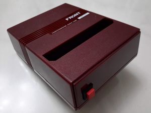
The Front Fareast (FFE) Super Magic Card (SMC-801) is FFE's last RAM cartridge, released in March 1991.
Capabilities:
- 512 KiB PRG DRAM, 8 KiB granularity
- 32 KiB WRAM, 8 KiB granularity
- 256 KiB CHR-RAM, 1 KiB granularity
- 16 KiB BIOS ROM
- Real-time save/restore state functionality
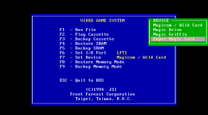
Games were available on 2.8" FDS floppy disks, on 3.5" MS-DOS FAT12 floppy disks in a custom FFE single-file format, or as a collection CD-ROM in the same custom FFE format to be uploaded via a DOS program to the SMC using a parallel port cable. Realtime save/restore is realized by bringing up the GUI during gameplay via pressing a red button on the SMC. The button status is polled by the BIOS' NMI handler.
The SMC plugs between the console and the FDS RAM Adapter. There are three modes of operation:
- Pass-through mode: SMC disabled;
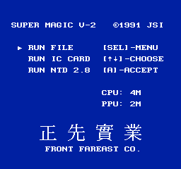
- GUI mode: for loading games and loading or saving save states;
- Play mode: for playing games.
Games converted to the iNES file format use Mappers 6, 8, 12 and 17 to denote various initial states of the SMC.
CPU Memory Layout
- GUI mode:
- CPU $5000-$5FFF: 4 KiB of scratch RAM
- CPU $6000-$7FFF: 8 KiB window into 32 KiB WRAM memory, or 8 KiB window into 512 KiB PRG memory
- CPU $8000-$BFFF: 16 KiB window into 512 KiB PRG memory
- CPU $C000-$FFFF: 16 KiB ROM BIOS
- PPU $0000-$1FFF: 8 KiB window into 256 KiB CHR memory
- Play mode:
- CPU $5000-$5FFF: 4 KiB of scratch RAM
- CPU $6000-$7FFF: 8 KiB window into 32 KiB WRAM memory
- CPU $8000-$FFFF: 32 KiB window into 512 KiB PRG memory
- PPU $0000-$1FFF: 8 KiB window into 256 KiB CHR memory
Banking modes in Play mode
Latch-based modes
- These modes are inherited from the Magic Card 1M and 2M, which had 128 KiB/256 KiB of PRG memory and only 32 KiB of CHR memory with 8 KiB granularity.
- A bus-conflict-free latch at CPU $8000-$FFFF switches PRG and CHR banks.
- The 1M Mode Register selects the latch-based mode.
- The latch is only active when PRG memory is write-protected.
0: UNROM
D~[.... .PPP]
         +++- CPU $8000-$BFFF: switchable 16 KiB PRG bank #0-#7 via PPP
              CPU $C000-$FFFF: fixed 16 KiB PRG bank #7
              PPU $0000-$1FFF: fixed 8 KiB CHR bank #0, writable
1: UN1ROM+CHRSW
D~[..BB BBCC]
     || ||++- PPU $0000-$1FFF: switchable 8 KiB CHR bank #0-#3 via CC, writable
     ++-++--- CPU $8000-$BFFF: switchable 16 KiB PRG bank #0-#15 via PPP
              CPU $C000-$FFFF: fixed 16 KiB PRG bank #7
UN1ROM+CHRSW is used for games that originally were SKROM with 128 KiB PRG and 128 KiB CHR data. The original 128 KiB CHR data are stored in the second 128 KiB of PRG address space, with a trainer program copying the most-recently-used CHR data into 32 KiB CHR memory.
2: UOROM
D~[.... PPPP]
        ++++- CPU $8000-$BFFF: switchable 16 KiB PRG bank #0-#15 via PPPP
              CPU $C000-$FFFF: fixed 16 KiB PRG bank #15
              PPU $0000-$1FFF: fixed 8 KiB CHR bank #0, writable
With no other means of masking PRG addresses, UNROM vs. UOROM are explicitly differentiated.
3: Reverse UOROM+CHRSW
D~[..CC PPPP]
     || ++++- CPU $C000-$FFFF: switchable 16 KiB PRG bank #0-#15 via PPPP
     ||       CPU $8000-$7FFF: fixed 16 KiB PRG bank #15
     ++------ PPU $0000-$1FFF: switchable 8 KiB CHR bank #0-#3 via CC, writable
4: GNROM
D~[..PP ..CC]
     ||   ++- PPU $0000-$1FFF: switchable 8 KiB CHR bank #0-#3 via CC, write-protected
     ++------ CPU $8000-$FFFF: switchable 32 KiB PRG bank #0-#3 via PP
5: CNROM-256
D~[.... ..CC]
          ++- PPU $0000-$1FFF: switchable 8 KiB CHR bank #0-#3 via CC, write-protected
              CPU $8000-$FFFF: fixed 32 KiB PRG bank #3
6: CNROM-128
D~[.... ...C]
           +- PPU $0000-$1FFF: switchable 8 KiB CHR bank #0-#1 via C, write-protected
              CPU $8000-$FFFF: fixed 32 KiB PRG bank #3
7: NROM-256
D~[.... ...C]
           +- PPU $0000-$1FFF: fixed 8 KiB CHR bank #0, write-protected
              CPU $8000-$FFFF: fixed 32 KiB PRG bank #3
With no other means of masking CHR addresses, CNROM-256 vs. CNROM-128 vs. NROM-256 are explicitly differentiated.
2M PRG banking mode
- Four registers at $8000-$9FFF/$A000-$BFFF/$C000-$DFFF/$E000-$FFFF switch four 8 KiB PRG banks and the common 8 KiB CHR bank. They overlap with the latch at $8000-$FFFF and accept values even when the 2M PRG banking mode itself is not active.
- 2M PRG banking mode is enabled via the 2M/4M Mode Register. When active, it overrides the Latch-based mode in all aspects except CHR memory protection, which is still decided by the 1M Mode Register.
- The entire 512 KiB can be reached on the Magic Card 4M and the Super Magic Card; the name follows the register's introduction in the Magic Card 2M.
D~[PPPP PPCC]
   |||| ||++- PPU $0000-$1FFF: switchable 8 KiB CHR bank #0-#3 via CC in $8000-$FFFF
   ++++-++--- CPU $8000-$9FFF: switchable 8 KiB PRG Bank #0-31 via PPPPPP in $8000-$9FFF
              CPU $A000-$BFFF: switchable 8 KiB PRG Bank #0-31 via PPPPPP in $A000-$BFFF
              CPU $C000-$DFFF: switchable 8 KiB PRG Bank #0-31 via PPPPPP in $C000-$DFFF
              CPU $E000-$FFFF: switchable 8 KiB PRG Bank #0-31 via PPPPPP in $E000-$FFFF
4M PRG banking mode
- Four registers at $4504-$4507 switch four 8 KiB PRG banks, while leaving the common 8 KiB CHR bank unaffected.
- They accept values even when the 4M PRG banking mode itself is not active. However, in that situation, they function as mirrors of the 2M banking mode's registers.
- 4M PRG banking mode is enabled via the 2M/4M Mode Register. When active, it overrides the Latch-based mode in all aspects except CHR memory protection, which is still decided by the 1M Mode Register.
- The entire 512 KiB can be reached.
D~[..PP PPPP]
     ++-++++- CPU $8000-$9FFF: switchable 8 KiB PRG Bank #0-63 via PPPPPP in $4504
              CPU $A000-$BFFF: switchable 8 KiB PRG Bank #0-63 via PPPPPP in $4505
              CPU $C000-$DFFF: switchable 8 KiB PRG Bank #0-63 via PPPPPP in $4506
              CPU $E000-$FFFF: switchable 8 KiB PRG Bank #0-63 via PPPPPP in $4507
1 KiB CHR banking mode
- Eight registers at $4510-$4517 switch eight 1 KiB CHR banks.
- When selected via $4500, four additional registers at $4518-$451B switch four 1 KiB CHR banks for nametables.
- 1 KiB CHR banking mode is enabled via the Super Magic Card mode register. When active, it overrides the CC bits that selected 8 KiB banks from 32 KiB.
D~[CCCC CCCC]
   ++++-++++- PPU $0000-$03FF: switchable 1 KiB CHR Bank #0-255 via CCCCCCC in $4510
              PPU $0400-$07FF: switchable 1 KiB CHR Bank #0-255 via CCCCCCC in $4511
              PPU $0800-$0BFF: switchable 1 KiB CHR Bank #0-255 via CCCCCCC in $4512
              PPU $0C00-$0FFF: switchable 1 KiB CHR Bank #0-255 via CCCCCCC in $4513
              PPU $1000-$13FF: switchable 1 KiB CHR Bank #0-255 via CCCCCCC in $4514
              PPU $1400-$17FF: switchable 1 KiB CHR Bank #0-255 via CCCCCCC in $4515
              PPU $1800-$1BFF: switchable 1 KiB CHR Bank #0-255 via CCCCCCC in $4516
              PPU $1C00-$1FFF: switchable 1 KiB CHR Bank #0-255 via CCCCCCC in $4517
              PPU $2000-$23FF: switchable 1 KiB CHR Bank #0-255 via CCCCCCC in $4518 when using CHR nametables
              PPU $2400-$27FF: switchable 1 KiB CHR Bank #0-255 via CCCCCCC in $4519 when using CHR nametables
              PPU $2800-$2BFF: switchable 1 KiB CHR Bank #0-255 via CCCCCCC in $451A when using CHR nametables
              PPU $2C00-$2FFF: switchable 1 KiB CHR Bank #0-255 via CCCCCCC in $451B when using CHR nametables
- The meaning of these registers changes when MMC4 mode is active. Because PPU A10 still selects between even and odd registers, each pair must hold the same value:
D~[CCCC CC..]
   ++++-++--- PPU $0000-$0FFF: switchable 4 KiB CHR Bank #0-63 via CCCCC in $4510 after reading from PPU $0FD8-$0FDF
              PPU $0000-$0FFF: switchable 4 KiB CHR Bank #0-63 via CCCCC in $4511 after reading from PPU $0FD8-$0FDF
              PPU $0000-$0FFF: switchable 4 KiB CHR Bank #0-63 via CCCCC in $4512 after reading from PPU $0FE8-$0FEF
              PPU $0000-$0FFF: switchable 4 KiB CHR Bank #0-63 via CCCCC in $4513 after reading from PPU $0FE8-$0FEF
              PPU $1000-$1FFF: switchable 4 KiB CHR Bank #0-63 via CCCCC in $4514 after reading from PPU $1FD8-$1FDF
              PPU $1000-$1FFF: switchable 4 KiB CHR Bank #0-63 via CCCCC in $4515 after reading from PPU $1FD8-$1FDF
              PPU $1000-$1FFF: switchable 4 KiB CHR Bank #0-63 via CCCCC in $4516 after reading from PPU $1FE8-$1FEF
              PPU $1000-$1FFF: switchable 4 KiB CHR Bank #0-63 via CCCCC in $4517 after reading from PPU $1FE8-$1FEF
Banking in GUI mode
In GUI mode, banking operates similarly to 4M mode:
D~[..PP PPPP]
     ++-++++- CPU $8000-$9FFF: switchable 8 KiB PRG Bank #0-63 via PPPPPP in $4504
              CPU $A000-$BFFF: switchable 8 KiB PRG Bank #0-63 via PPPPPP in $4505
              CPU $6000-$7FFF: switchable 8 KiB PRG Bank #0-63 via PPPPPP in $4507 (see below)
- When PRG memory is write-protected via the the 1M banking mode register, CPU $6000-$7FFF is an 8 KiB window into 32 KiB WRAM banked via register $4500.
- When PRG memory is write-enabled via the the 1M banking mode register, CPU $6000-$7FFF is an 8 KiB window into 512 KiB PRG DRAM banked via register $4507.
Registers
1M banking mode ($42FC-$42FF, write-only)
A~FEDC BA98 7654 3210  D~7654 3210
  -------------------    ---------
  0100 0010 1111 11bM    BBBM ....
                   |+----|||+------ Set nametable mirroring type
                   |     |||         0: One-screen, page 0
                   |     |||         1: One-screen, page 1
                   |     |||         2: Vertical
                   |     |||         3: Horizontal
                   +-----|||------- 0: PRG memory is writeable, latch is disabled
                         |||        1: PRG memory is write-protected, latch is enabled
                         +++------- Select latch-based banking mode
2M/4M PRG banking mode ($43FC-$43FF, write-only)
A~FEDC BA98 7654 3210  D~7654 3210
  -------------------    ---------
  0100 0011 1111 11NM    .... ..CC
                   ||           ++- switchable 8 KiB CHR bank #0-#3 via CC
                   ||
                   |+- 2M and 4M PRG banking mode select
                   |    0: Enable
                   |    1: Disable
                   +-- 2M or 4M banking mode select if M=0
                        0: 4M banking mode
                        1: 2M banking mode
The CC bits are mirrors of those in the latch at $8000-$FFFF.
Super Magic Card mode ($4500, write-only)
D~7654 3210
  ---------
  PMWW ImNC
  |||| |||+- CHR-RAM mode
  |||| |||    0: 8 KiB
  |||| |||    1: 1 KiB
  |||| ||+-- Nametable mode
  |||| ||     0: Nametables from CHR memory via $4518-$451C
  |||| ||     1: Nametables from CIRAM, subject to mirroring via $42FC-$42FF
  |||| |+--- MMC4 mode
  |||| |      0: Enabled (ignored when C=0)
  |||| |      1: Disabled
  |||| +---- Play mode: IRQ source select
  ||||        0: M2 rise
  ||||        1: PA12 rise (unfiltered, e.g. 8 rises per scanline)
  ||||       GUI mode: Data source select
  ||||        0: Parallel port
  ||||        1: Floppy disk controller
  ||++------ Select 8 KiB WRAM bank at CPU $6000-$7FFF
  |+-------- Memory map
  |           0: GUI mode
  |           1: Play mode
  +--------- Pass-through mode
              0: Disabled
              1: Enabled, pass through all signals from cartridge connector
The floppy disk controller is held in a reset state while the parallel port is selected via D3.
State register 1 ($4500, read-only)
D~7654 3210
  ---------
  WBLL LMPm
  |||| |||+- Current mirroring type, i.e. A0 of register $42Fx
  |||| ||+-- PRG memory write-protection status, i.e. A1 of register $42Fx
  |||| |+--- Current mirroring setting, i.e. D4 of register $42Fx
  ||++-+---- Current latch-based mode, i.e. D5-D7 of register $42Fx
  |+-------- 0: Button pressed
  +--------- 1: Byte waiting to be read from parallel port
State register 2 ($4501, read-only)
D~7654 3210
  ---------
  LLLL LL42
  |||| |||+- 2M PRG banking mode status, i.e. A0 of register $43Fx
  |||| ||+-- 4M PRG banking mode status, i.e. A1 of register $43Fx
  ++++-++--- Current latch value for latch-based modes
Parallel port/Floppy disk controller ($4508-$450F, read/write)
When the floppy disk controller is enabled via $4500, these are the registers of an Intel 82077A-compatible floppy disk controller:
$4508: Status Register A
$4509: Status Register B (unused)
$450A: Digital Output Register
$450B: Tape Drive Register (unused)
$450C: Main Status Register (read)/Data Rate Select Register (write)
$450D: Data Register
$450F: Digital Input Register (unused)
The floppy disk controller's DMA and IRQ facilities are not used. During a floppy disk operation, BIOS continuously polls the status and transmits data byte-for-byte via these registers.
When the floppy disk controller is disabled via $4500, $4508-$450F becomes a simple input/output port for the RAM cartridge's parallel port.
FDS Write Data ($4024)
This register is not part of the RAM cartridge, but part of the FDS RAM adapter that originally attached to it. Because the Magic Card 1M and 2M, the predecessors to the Super Magic Card, had no IRQ counter of its own, a few games abuse the FDS Disk Data IRQ for frame timing and write any value to this register to acknowledge a pending IRQ.
FDS Control ($4025)
This register is not part of the RAM cartridge, but part of the FDS RAM adapter that originally attached to it. Because the Magic Card 1M and 2M, the predecessors to the Super Magic Card, had no IRQ counter of its own, a few games abuse the FDS Disk Data IRQ for frame timing. If bit 7 is set, the FDS RAM adapter will generate IRQs every 1,792 cycles of the 21.4772 MHz master clock, or after every 149+1/3 CPU cycles.
IRQ Disable ($4501, write-only)
Acknowledges a pending IRQ and disables counting.
IRQ Counter LSB/MSB ($4502/$4503, write-only)
- This upwards-counting signed 16-bit counter is increased on every M2 or PA12 rise and raises an IRQ when flipping frmo $FFFF to $0000.
- Writing to either register acknowledges a pending IRQ.
- Writing to $4503 enables counting and IRQ generation.
Scratch RAM ($5000-$5FFF)
Certain locations in scratch RAM are continuously updated with the cached values of write-only registers to aid realtime state saving:
$5000-$5015: Cached values of APU registers $4000-$4015
$5500-$501F: Cached values of SMC registers $4500-$451F
$5800-$5807: Cached values of PPU registers $2000-$2007
Remote Control
The Super Magic Card can be remotely controlled via the parallel port. This functionality is used by FFE's "VGS.EXE" MS-DOS software, which allows uploading games via the parallel port from an MS-DOS computer and downloading real-time states. The remote program must send a command of the following format:
D5 AA 96 nn aa aa ll ll cc ... cc
         || || || || || ||     ++- Checksum over data
         || || || || || ++-------- Checksum over nn aa aa ll ll
         || || || ++-++----------- Data length LSB MSB
         || ++-++----------------- Target address LSB MSB
         ++----------------------- Command#
The following command numbers are recognized:
00  Upload data into CPU address space
01  Download data from CPU address space
02  Upload data into PPU address space
03  Download data from PPU address space
04  JMP to specified address
05  Special function. Target address is the special function number, length is 0.
    0       Reset SMC
    1       Run game in DRAM
    2       Switch to pass-through mode
    3       Pause
    4       Continue
    5       Abort current operation
06  Unknown
SMC will respond to a successful command by sending byte $04 meaning "acknowledge", or $00 meaning "failure". The checksum function is a simple XOR of all bytes, finally XOR'd with $81.
There is no high-level "upload/download game/save file" command; instead, a remote program must know from where the various cached register values must be requested or where they must be stored.


