Famicom cartridge dimensions: Difference between revisions
mNo edit summary |
m (Add category) |
||
| (12 intermediate revisions by the same user not shown) | |||
| Line 23: | Line 23: | ||
== Famicom cartridge PCB outline == | == Famicom cartridge PCB outline == | ||
These outlines of different cartridge PCB types are based on the most space-filling variant, so that designers may choose to cut off unused portions that their designs may not need. Some outlines of cartridges with no maximally space filling PCB are thus modified to be such, with measurements being based on adjacent types made by the same producer. | |||
Each cartridge type varies in how the 60 pin card edge is implemented. The pin pitch is 2.54mm, with 2 rows of 30 pads. Each pad may be uniform in dimensions, or slightly thicker and longer for power/ground. | |||
Each cartridge type varies in how the 60 pin card edge is implemented. The pin pitch is 2.54mm, with 2 rows of 30 pads. Each pad may be uniform in dimensions, or slightly thicker and longer for power/ground. This outline is based on measurements from a HVC-TGROM-01 cartridge, with bigger | |||
[[File:HVC-TGROM-01- | === HVC-Ax/Fx/Px/Sx/TxROM (MMC1-4 mapper boards) === | ||
This outline is based on measurements from a HVC-TGROM-01 type cartridge PCB, compatible with any cartridge shell that supports any HVC-Ax/Fx/Px/Sx/TxROM PCB or similar/bigger. These measurements are measured with vernier calipers with 0.05 mm accuracy. Note that this outline also details where the soldermask ends for the card edge. | |||
[[File:HVC-TGROM-01-board.svg|frame|center|Technical drawing of the outlines of an HVC-TGROM-01 type cartridge PCB.]] | |||
{| class="wikitable" align="center" style="margin: auto;" | |||
!colspan="3"|Dimensions | |||
|- | |||
|Designator ||Dimensions in mm (±0.05 mm) ||Description | |||
|- | |||
|A ||90 ||Board width | |||
|- | |||
|A.1 ||78.4 ||Card edge width | |||
|- | |||
|A.2 ||81 ||Notched width | |||
|- | |||
|A.2.1 ||43 ||Inset board width 1 | |||
|- | |||
|A.2.2 ||33 ||Inset board width 2 | |||
|- | |||
|B ||46.1 ||Board height | |||
|- | |||
|B.1 ||23.2 ||Inset board height 1 | |||
|- | |||
|B.2 ||20.9 ||Inset board height 2 | |||
|- | |||
|B.3 ||10.7 ||Card edge depth | |||
|- | |||
|C ||1.2 ||Board thickness | |||
|- | |||
|D.1 ||3 ||Card edge base to pad top | |||
|- | |||
|D.2 ||4 ||Card edge base to soldermask keepout | |||
|- | |||
|D.3 ||6.7 ||Power pad height | |||
|- | |||
|D.4 ||5.7 ||Signal pad height | |||
|- | |||
|E.1 ||0.57 ||Power pad to card edge side | |||
|- | |||
|E.2 ||1.57 ||Signal pad to card edge side | |||
|- | |||
|E.3 ||2.6 ||Power pad width | |||
|- | |||
|E.4 ||1.6 ||Signal pad width | |||
|- | |||
|E.5 ||0.94 ||Space between pads | |||
|- | |||
|E.6 ||2.54 ||Pad spacing | |||
|} | |||
=== HVC-ExROM === | === HVC-ExROM === | ||
''TODO: measure and publish dimensions'' | ''TODO: measure and publish dimensions'' | ||
=== HVC- | === HVC-N/Cx/Gx/UxROM 01-05 (discrete mapper boards) === | ||
This outline is based on measurements from a HVC-CNROM-256K-01 type cartridge PCB, augmented with dimensions from a HVC-TGROM-01 type PCB. This is compatible with any cartridge shell that supports any HVC-N/Cx/Gx/UxROM 01-05 PCB or similar/bigger. These measurements are measured with vernier calipers with 0.05 mm accuracy. Note that this outline also details where the soldermask ends for the card edge. | |||
[[File:HVC-CNROM-256K-01-board.svg|frame|center|Technical drawing of the outlines of an augmented HVC-CNROM-256K-01 type cartridge PCB.]] | |||
{| class="wikitable" align="center" style="margin: auto;" | |||
!colspan="3"|Dimensions | |||
|- | |||
|Designator ||Dimensions in mm (±0.05 mm) ||Description | |||
|- | |||
|A ||90 ||Board width | |||
|- | |||
|A.1 ||78.4 ||Card edge width | |||
|- | |||
|A.2 ||68 ||Notched width | |||
|- | |||
|A.2.1 ||31.5 ||Inset board width 1 | |||
|- | |||
|A.2.2 ||26.5 ||Inset board width 2 | |||
|- | |||
|A.3 ||39.5 ||Hole 1 to board edge | |||
|- | |||
|A.4 ||1/2 of A ||Hole 2 to board edge | |||
|- | |||
|A.5 ||3 ||Hole 1 diameter | |||
|- | |||
|A.6 ||5 ||Hole 2 diameter | |||
|- | |||
|B ||46.1 ||Board height | |||
|- | |||
|B.1 ||23.2 ||Inset board height 1 | |||
|- | |||
|B.2 ||20.9 ||Inset board height 2 | |||
|- | |||
|B.3 ||10.7 ||Card edge depth | |||
|- | |||
|B.4 ||19.8 ||Hole 1 center height | |||
|- | |||
|B.5 ||10.3 ||Hole 2 center height | |||
|- | |||
|C ||1.2 ||Board thickness | |||
|- | |||
|D.1 ||3 ||Card edge base to pad top | |||
|- | |||
|D.2 ||4 ||Card edge base to soldermask keepout | |||
|- | |||
|D.3 ||6.7 ||Power pad height | |||
|- | |||
|D.4 ||5.7 ||Signal pad height | |||
|- | |||
|E.1 ||0.57 ||Power pad to card edge side | |||
|- | |||
|E.2 ||1.57 ||Signal pad to card edge side | |||
|- | |||
|E.3 ||2.6 ||Power pad width | |||
|- | |||
|E.4 ||1.6 ||Signal pad width | |||
|- | |||
|E.5 ||0.94 ||Space between pads | |||
|- | |||
|E.6 ||2.54 ||Pad spacing | |||
|} | |||
[[Category:Hardware]] | |||
Latest revision as of 15:34, 18 September 2022
This page documents the dimensions of common Famicom cartridges, including their cartridge shell and their corresponding PCB type. The source files are open-source and available on Github.
TODO: identify more cartridge shell forms
Famicom cartridge shell outline
Small cartridge form
HVC-TxROM
TODO: measure and publish dimensions
HVC-NROM/CNROM
TODO: measure and publish dimensions
Large cartridge form
HVC-ExROM
TODO: measure and publish dimensions
Miscellaneous cartridge forms
TODO: document and measure other forms
Famicom cartridge PCB outline
These outlines of different cartridge PCB types are based on the most space-filling variant, so that designers may choose to cut off unused portions that their designs may not need. Some outlines of cartridges with no maximally space filling PCB are thus modified to be such, with measurements being based on adjacent types made by the same producer.
Each cartridge type varies in how the 60 pin card edge is implemented. The pin pitch is 2.54mm, with 2 rows of 30 pads. Each pad may be uniform in dimensions, or slightly thicker and longer for power/ground.
HVC-Ax/Fx/Px/Sx/TxROM (MMC1-4 mapper boards)
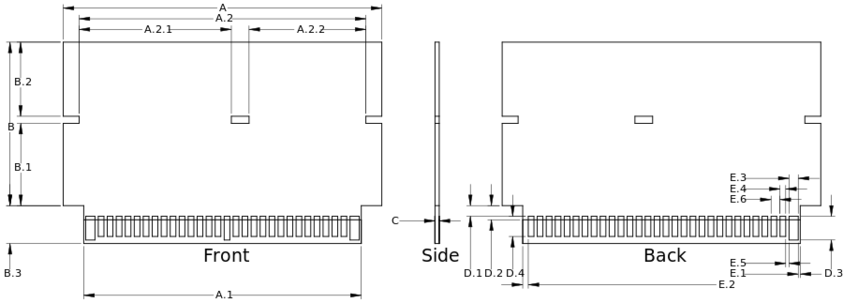
This outline is based on measurements from a HVC-TGROM-01 type cartridge PCB, compatible with any cartridge shell that supports any HVC-Ax/Fx/Px/Sx/TxROM PCB or similar/bigger. These measurements are measured with vernier calipers with 0.05 mm accuracy. Note that this outline also details where the soldermask ends for the card edge.
| Dimensions | ||
|---|---|---|
| Designator | Dimensions in mm (±0.05 mm) | Description |
| A | 90 | Board width |
| A.1 | 78.4 | Card edge width |
| A.2 | 81 | Notched width |
| A.2.1 | 43 | Inset board width 1 |
| A.2.2 | 33 | Inset board width 2 |
| B | 46.1 | Board height |
| B.1 | 23.2 | Inset board height 1 |
| B.2 | 20.9 | Inset board height 2 |
| B.3 | 10.7 | Card edge depth |
| C | 1.2 | Board thickness |
| D.1 | 3 | Card edge base to pad top |
| D.2 | 4 | Card edge base to soldermask keepout |
| D.3 | 6.7 | Power pad height |
| D.4 | 5.7 | Signal pad height |
| E.1 | 0.57 | Power pad to card edge side |
| E.2 | 1.57 | Signal pad to card edge side |
| E.3 | 2.6 | Power pad width |
| E.4 | 1.6 | Signal pad width |
| E.5 | 0.94 | Space between pads |
| E.6 | 2.54 | Pad spacing |
HVC-ExROM
TODO: measure and publish dimensions
HVC-N/Cx/Gx/UxROM 01-05 (discrete mapper boards)
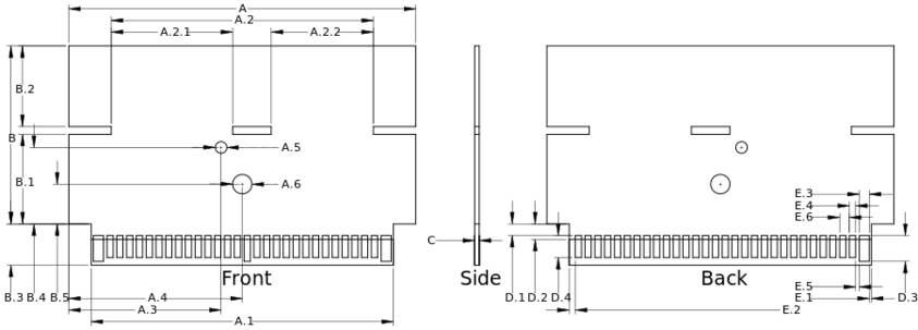
This outline is based on measurements from a HVC-CNROM-256K-01 type cartridge PCB, augmented with dimensions from a HVC-TGROM-01 type PCB. This is compatible with any cartridge shell that supports any HVC-N/Cx/Gx/UxROM 01-05 PCB or similar/bigger. These measurements are measured with vernier calipers with 0.05 mm accuracy. Note that this outline also details where the soldermask ends for the card edge.
| Dimensions | ||
|---|---|---|
| Designator | Dimensions in mm (±0.05 mm) | Description |
| A | 90 | Board width |
| A.1 | 78.4 | Card edge width |
| A.2 | 68 | Notched width |
| A.2.1 | 31.5 | Inset board width 1 |
| A.2.2 | 26.5 | Inset board width 2 |
| A.3 | 39.5 | Hole 1 to board edge |
| A.4 | 1/2 of A | Hole 2 to board edge |
| A.5 | 3 | Hole 1 diameter |
| A.6 | 5 | Hole 2 diameter |
| B | 46.1 | Board height |
| B.1 | 23.2 | Inset board height 1 |
| B.2 | 20.9 | Inset board height 2 |
| B.3 | 10.7 | Card edge depth |
| B.4 | 19.8 | Hole 1 center height |
| B.5 | 10.3 | Hole 2 center height |
| C | 1.2 | Board thickness |
| D.1 | 3 | Card edge base to pad top |
| D.2 | 4 | Card edge base to soldermask keepout |
| D.3 | 6.7 | Power pad height |
| D.4 | 5.7 | Signal pad height |
| E.1 | 0.57 | Power pad to card edge side |
| E.2 | 1.57 | Signal pad to card edge side |
| E.3 | 2.6 | Power pad width |
| E.4 | 1.6 | Signal pad width |
| E.5 | 0.94 | Space between pads |
| E.6 | 2.54 | Pad spacing |

