File:Apu address.jpg
Original file (1,314 × 400 pixels, file size: 294 KB, MIME type: image/jpeg)
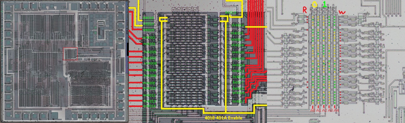
The NES APU's address decoder, generating enables for all reads/writes within $4000-$401F.
Of very special note are the 4 signals at the very top for readable registers at $4018 (pulse 0 output on D0-D3 and pulse 1 output on D4-D7), $4019 (triangle output on D0-D3, noise output on D4-D7), $401A (DPCM output on D0-D6), and a writable register at $401A (set triangle position to D0-D4, and lock channel outputs using D7); all 4 of these signals have an additional enable which seems to come from the vicinity of pin 30.
Source: http://uxul.org/~noname/chips/cpu-5/stitched/final/ http://uxul.org/~noname/chips/cpu-2/no-metal/stitched/final/
File history
Click on a date/time to view the file as it appeared at that time.
| Date/Time | Thumbnail | Dimensions | User | Comment | |
|---|---|---|---|---|---|
| current | 21:56, 21 September 2021 | 1,314 × 400 (294 KB) | >Maintenance script | == Summary == Importing file |
You cannot overwrite this file.
File usage
There are no pages that use this file.