UNROM 512
UNROM 512 is a discrete-logic board made by RetroUSB as an extension of UNROM with up to 512kB of PRG ROM, bankable CHR RAM, an option for mapper-controlled single-screen mirroring, as well as a self-flashable configuration for rewriting PRG. Games that use this board include Study Hall and Battle Kid 2: Mountain of Torment. Since it's initial creation InfiniteNesLives has replicated it's design and also added an optional four-screen mirroring variation.
The iNES format assigns iNES Mapper 030 to UNROM 512.
The UNIF names for this board are UNROM-512-8, UNROM-512-16 and UNROM-512-32, depending on how much CHR RAM is present.
Overview
- PRG ROM size: Up to 512kB (Up to 256kB on 8Bit XMAS)
- PRG ROM bank size: 16kB
- PRG RAM: None
- CHR capacity: Up to 32kB RAM
- CHR bank size: 8kB
- Nametable mirroring: Solder pads select vertical, horizontal, mapper-controlled one-screen. (InfiniteNesLives variation permits four-screen mirroring)
- Subject to bus conflicts: Yes, in the non-flashable configuration
Board
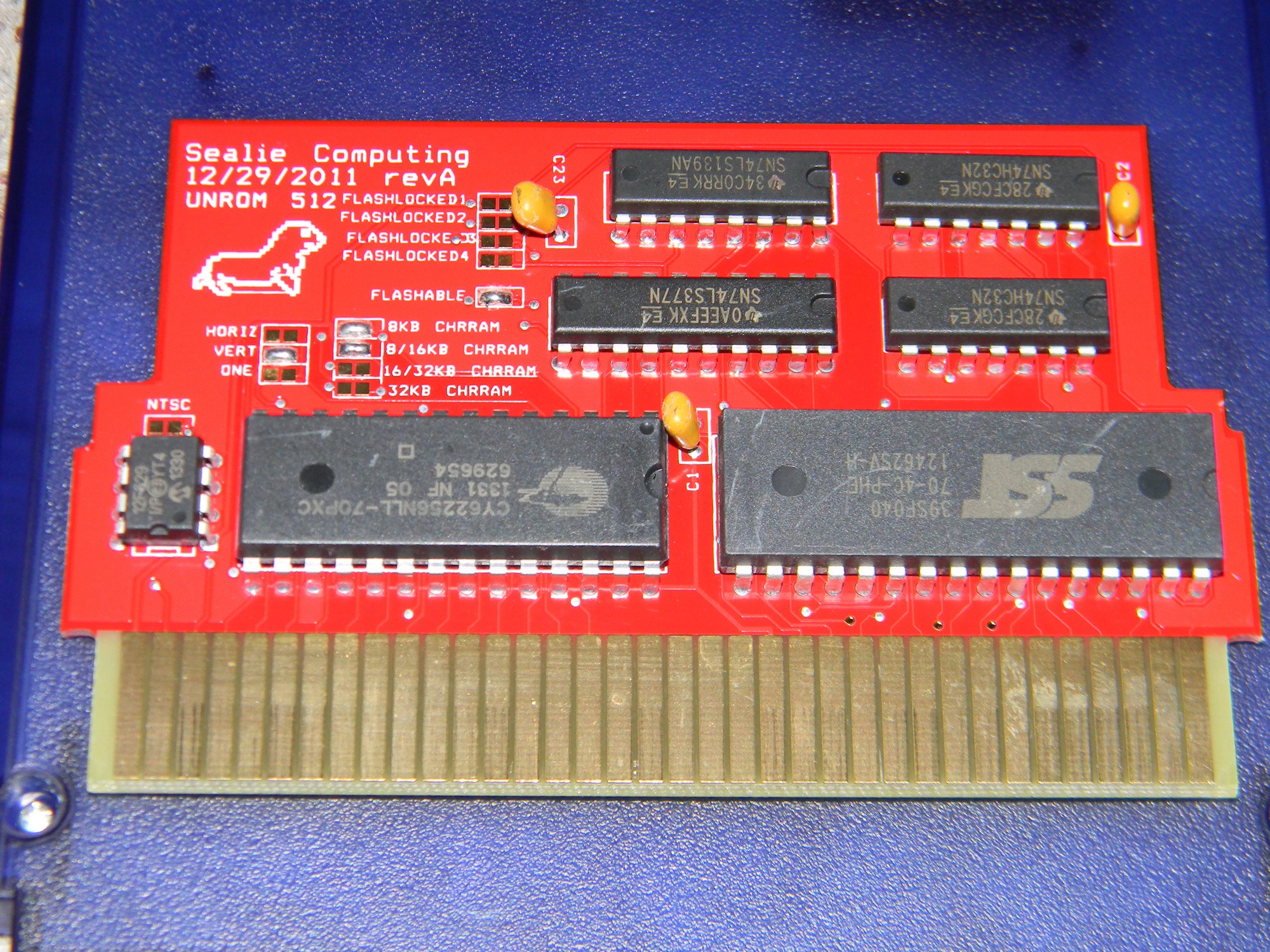
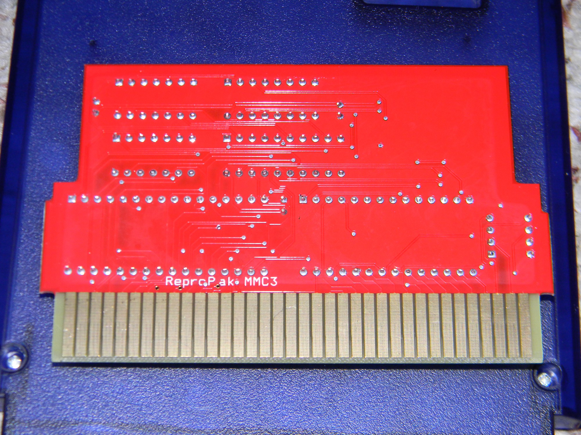
The example board in question is marked as follows: "Sealie Computing", "12/29/2011 revA", "UNROM 512". The backside of the board was mislabeled with "ReproPak MMC3".
The board includes 4x banks worth of full 8kB CHR-RAM (Configurable by jumpers) and 32x 16kB PRG banks.
The board can be wired in a non-flashable or self-flashable configurations.
Mirroring can be selected between Horizontal, Vertical, and Mapper-controlled One Screen. The InfiniteNesLives variation optionally adds 4-screen mirroring capabilities.
Bus conflicts are only present on the non-flashable configuration of the board.
Some images of the board:
- Study Hall PCB Front
- Battle Kid 2 PCB Front
- PCB Back
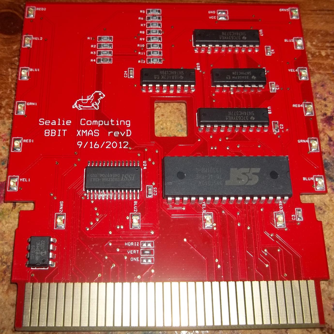
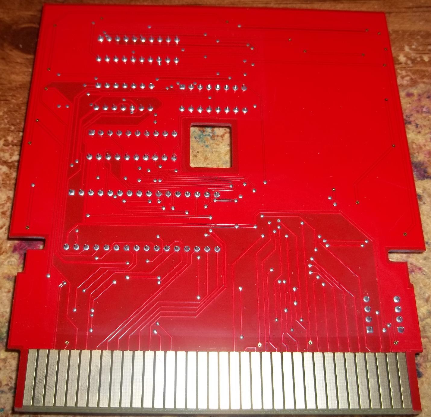
- 8BIT XMAS revD PCB Front
- 8BIT XMAX revD PCB Back
When board is not flashable:
  Registers:
  ---------------------------

  Range,Mask:   $8000-FFFF, $8000

    $8000:  [MCCP PPPP]
      M = One screen Mirroring select
      C = CHR RAM bank
      P = PRG ROM bank

  PRG Setup:
  ---------------------------
       $8000   $A000   $C000   $E000
      +-------------------------------+
      |     $8000     |     { -1}     |
      +---------------+---------------+

  CHR Setup:
  ---------------------------
        $0000   $1000
      +-------+-------+
      |     $0000     |
      +-------+-------+
When board is self flashable:
  Registers:
  ---------------------------

  Range,Mask:   $8000-BFFF, $8000
                $C000-FFFF, $C000

    $8000:  [.... ....]
      Write a sequence of bytes here for writing to the flash. The sequence is as follows

(This code must exist in wram):
        Erase 4KB Flash Sector:
        $C000:$01, $9555:$AA
        $C000:$00, $AAAA:$55
        $C000:$01, $9555:$80
        $C000:$01, $9555:$AA
        $C000:$00, $AAAA:$55
        $C000:BANK, ADDR:$30 (Where BANK is $00-1F, ADDR is $8000,$9000,$A000,$B000)
        Read the written location twice until you get $FF twice.

        Write a byte:
        $C000:$01, $9555:$AA
        $C000:$00, $AAAA:$55
        $C000:$01, $9555:$A0
        $C000:BANK, ADDR:DATA (Where BANK is $00-1F, ADDR is $8000-$BFFF, DATA is $00-$FF)
        Read the written location twice until you get DATA twice.

Additionally, on 8Bit XMAS boards, any writes here controls the LEDs as follows.

    $8000:  [BYGR bygr]
        B = Blue 3, Blue 4
        Y = Yellow 3, Yellow 4
        G = Green 3, Green 4
        R = Red 3, Red 4
        b = Blue 1, Blue 2
        y = Yellow 1, Yellow 2
        g = Green 1, Green 2
        r = Red 1, Red 2


    $C000:  [MCCP PPPP]
      M = One screen Mirroring select
      C = CHR RAM bank
      P = PRG ROM bank

  PRG Setup:
  ---------------------------
       $8000   $A000   $C000   $E000
      +-------------------------------+
      |     $8000     |     { -1}     |
      +---------------+---------------+

  CHR Setup:
  ---------------------------
        $0000   $1000
      +-------+-------+
      |     $8000     |
      +-------+-------+
Here's a schematic of the board:
             ____
A14 ---------\    \
              )    >--- ROM A14
377 Q0 ------/____/

             ____
A14 ---------\    \
              )    >--- ROM A15
377 Q1 ------/____/

             ____
A14 ---------\    \
              )    >--- ROM A16
377 Q2 ------/____/

             ____
A14 ---------\    \
              )    >--- ROM A17
377 Q3 ------/____/

             ____
A14 ---------\    \
              )    >--- ROM A18
377 Q4 ------/____/

16/32KB CHRRAM
377 Q5 --[]--+-- CHRRAM A13
             |
VCC -----[]--+
8KB CHRRAM

8/16KB CHRRAM
VCC -----[]--+
             |
377 Q6 --[]--+-- CHRRAM A14
32KB CHRRAM

ONE
377 Q7 --[]--+
             |
VERT         |
PPU A10 -[]--+-- CIRAM_A10
             |
HORIZ        |
PPU A11 -[]--+

FLASHLOCKED3
R/W ------[]-+
             |
FLASHABLE    |
GND ------[]-+-- 377_/CE

FLASHLOCKED1
VCC ------[]-------+
          ½74LS139 |
          .------. |
CPUA14----|A   Y0|-+- PRGROM_/WE
R/W ------|B   Y1|-+- 377_CLK
          |    Y2| |
/ROMSEL-+-|G   Y3| |
        | '------' |
        |          |
        +---[]-----+
       FLASHLOCKED2

FLASHLOCKED4
GND ------[]-----+
        ½74LS139 |
        .------. |
R/W ----|A   Y0| |
GND ----|B   Y1|-+- PRGROM_/OE
        |    Y2|
/ROMSEL-|G   Y3|
        '------'

With 8Bit Xmas Board, there is a second 377 chip for the LEDs, and 2 jumpers to control whether the 377 is sourcing
current to the LEDs or sinking current from them.  Additionally, the board has no flash control jumpers, and is hard-wired
flashable,  and has no CHR ram control jumpers, is hard-wired as 32KB, and it does not have the second 74LS32 chip,
required for a 512KB board, so its max size is 256KB.

Q0-----R1-----RED1-----RED2-------+
Q1--+--R6-----GRN1----------------+
    +--R5-----GRN2----------------+
Q2-----R3-----YEL1-----YEL2-------+
Q3--+--R9-----BLU1----------------+
    +--R10----BLU2----------------+
Q4-----R2-----RED3-----RED4-------+
Q5--+--R7-----GRN3----------------+
    +--R8-----GRN4----------------+
Q6-----R4-----YEL3-----YEL4-------+
Q7--+--R11----BLU3----------------+
    +--R12----BLU4----------------+
                                  |
VCC---------[]--------------------+
GND---------[]--------------------+
The board is wired in one of the following configurations:
Not Flashable:
- All 4 Flash Locked jumpers are soldered.
- Flashable jumper is not soldered.
- 74*139 is not mounted.
- This configuration is subject to bus conflicts
Flashable:
- All 4 Flash Locked jumpers are not soldered.
- Flashable jumper is soldered.
- 74*139 is mounted.
- This configuration is not subject to bus conflicts
The Self-flashable configuration should be implemented according to the SST39SF040's datasheet.
Example flash writing code - Flash.asm
InfiniteNesLives four-screen mirroring variation:
- Two of the unused OR gates are used in combination with jumpers to disable NES mainboard VRAM/CIRAM and utilize cartridge VRAM for all pattern, name, & attribute tables.
- This variation only allows CHR-RAM size of 32KB, however the last CHR-RAM bank is designated for non-pattern table use.
- - This restricts the user to only having free use of the first 3 CHR-RAM banks (24KB) for pattern table tile data.
- The last 8KB CHR-RAM bank are mapped to PPU $2000-3FFF (effectively $2000-3F00 due to palette data.)
- The first 4KB of this last CHR-RAM bank is mapped to PPU $2000-2FFF to provide four-screen mirroring.
- PPU $3000-3EFF are no longer mirrors to nametables, and actually have RAM mapped to each byte which aren't used by the PPU for rendering.
- - This 3.75KB of RAM can be used by the developer as a 'scratch RAM' space only accessible via CPU $2006/2007.
- - The last 256bytes of the last CHR-RAM bank are not normally accessible due to pallette data being mapped to PPU $3F00-3FFF.
- Setting of both CHR RAM bank bits ($8000: 0bx11xxxxx) is permissible, but extreme care must be used when the PPU is rendering as it has the effect of mapping the last CHR-RAM bank to both PPU $0000-1FFF (Pattern tables), and PPU $2000-3F00 (Name/Attribute tables) at the same time.
- - Improperly operating in this mode will render NT/AT data as tiles in PT0, and writes to PT0 will corrupt NT/AT data.
- - This mode is the only means of gaining access to the last 256bytes of the last CHR-RAM bank which are normally hidden behind PPU pallette address space.
PPU memory map:
| Address range | Size | Description |
|---|---|---|
| $0000-$0FFF | $1000 | Pattern Table 0 |
| $1000-$1FFF | $1000 | Pattern Table 1 |
| $2000-$23FF | $0400 | Nametable 0 |
| $2400-$27FF | $0400 | Nametable 1 |
| $2800-$2BFF | $0400 | Nametable 2 |
| $2C00-$2FFF | $0400 | Nametable 3 |
| $3000-$3EFF | $0F00 | Scratch RAM |
| $3F00-$3F1F | $0020 | Palette RAM indexes |
| $3F20-$3FFF | $00E0 | Mirrors of $3F00-$3F1F |
Electrical Schematic:
             ____
PPU A13 -----\    \
              )    >--- CHRRAM A13
377 Q5 ------/____/

             ____
PPU A13 -----\    \
              )    >--- CHRRAM A14
377 Q6 ------/____/

NON-4SCREEN
PPU A13 ----[]--+
                |
GND --------[]--+---- CHRRAM /CE (Cartridge VRAM)
4SCREEN MIRROR

NON-4SCREEN
PPU /A13 ---[]--+
                |
VCC --------[]--+---- CIRAM /CE (NES mainboard VRAM)
4SCREEN MIRROR
Mapper
NES 2.0 may specify the CHR-RAM size from 8 to 32 kB, but the default for iNES should to use 32 kB.
If the Battery flag is set, which indicates the mapper is flashable, then no bus conflicts should be emulated. On the other hand, bus conflicts should be emulated if the battery flag is cleared.
Mapper controlled one-screen mirroring is only emulated if the Four-Screen mirroring flag is set, otherwise, it is hard-locked on either horizontal or vertical mirroring. This needs to be officially disambiguated in order to define how to differentiate between one-screen and four-screen. Utilization of the Four-Screen mirroring flag to denote one-screen mirroring does not follow logically from the nes 2.0 header definition.
Mapper 30 is currently only using sub mapper 0. The other sub mappers are reserved for future use.
Supported in FCEUX as of r3071, Supported in BizHawk as of r6322